Following my recent post regarding IoT security: Firmware Dump I would like to show you today how to use JTAgulator to identify JTAG pinouts to them use it for for hacking and exploitation.
JTAG is a standard interface present on printed circuit boards (PCBs) used to interact with an integrated circuit. It was developed on 1990 and originally used for testing integrated circuits. As PCBs grew in complexity and density it started to become very difficult for testing it due to physical limitations or even loss of physical access to signals.
That’s when JTAG/boundary-scan came as an elegant solution for this issue. Today, JTAG is used for everything from testing interconnects and functionality on ICs to programming flash memory of systems deployed in the field and everything in-between.
It’s a wonderful solution but also a great resource for hackers. From a security perspective JTAG is used mostly to:
- Manipulate individual pins on components
- Change component state
- Alter flash memory
- Get access to many debug utilities
Typically JTAG uses 5 signals:
- TDI – Test Data In, the input from the debugger
- TDO – Test Data Out, the return end of the chain
- TCK – Test Clock, clocks this data along synchronously, similarly to SPI
- TMS – Test Mode Select, lets the devices know that they’re being debugged — it’s a global chip select
- TRST – Test Reset, an optional signal that resets all devices in the chain

Now, to identify the JTAG pins you will need to do a pin count, trace known JTAG lines out of the IC, do some good guesses or test them. For example, the ground pins are easy to identify with a continuity tester.
In many cases those things won’t be enough and you won’t be able to easily identify the JTAG pins. Maybe because the designer is not following any standard, or because they want to obfuscate, and here is where the JTAGulator takes place. It’s a very smart device that mainly brute-force and test all the pins and identify them for you. If you are interested in know more about it, read Joe’s slides from his DEFCON talk (PDF).

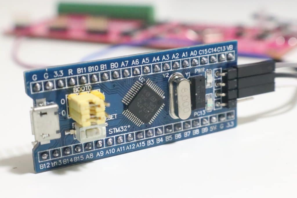
So now it’s time to put our hands dirty to see how this works. Let’s try to use JTAGulator to identify the JTAG pinouts of a STM32 chip from a small dev board.
As soon as you had identified your JTAG pins from the PCB you connect them to the JTAGulator using proper wiring. On my case I will needed female to female wiring. It’s important to interconnect the Gnd pins from both your target PCB and the JTAGulator. The other pins don’t really matter how you connect to your JTAGulator. The tests it will run will identify them for you.

Power both of your PCBs and connect the JTAGulator to your system. Once connected set the bound rate to 115200 using the following command:
sudo screen /dev/ttyUSB0 115200
If you’re using a different system the device could be named differently and instead of /dev/ttyUSB0 you will have to replace it to the name of your device.
When you get the prompt, use “V” to set the voltage and “B” to let JTAGulator identify the pins for you.

Also check the video below for more information. And now that you know the pinout you will be able start doing JTAG exploitation to read the entire content of the chip, upload malware and much more but I will let this for a future post.
See also: IoT Security: Firmware Dump